My Smart Switch, or How I Built a Smarthome Gadget with No Electronics Experience, While Living in a Village in Indonesia
by kacang bawang
They say that laziness is the mother of progress. It certainly was in my case. I am currently residing in Indonesia, where the outside lighting of one’s house is somewhat of a security practice, and it so happened that it became my job to ensure that these lights went on every evening, and equally importantly, off every morning. This involved making a trip around the perimeter of the house each evening and flipping all the light switches I came across. It is especially hard to remember to do this in the morning, because the sunlight makes it is hard to see that the lights are on. Sure enough, after about a week I no longer saw the joy in this daily routine and decided to do something about it. I was going to make a remote-controlled switch that would automate this task, and at the same time, become the foundation of a smart home installation I’ve been dreaming about. There was only one little problem – I knew absolutely nothing about designing electronics and PCBs.
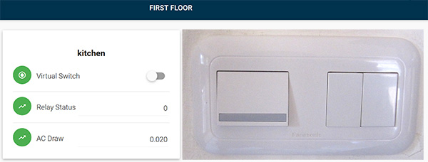
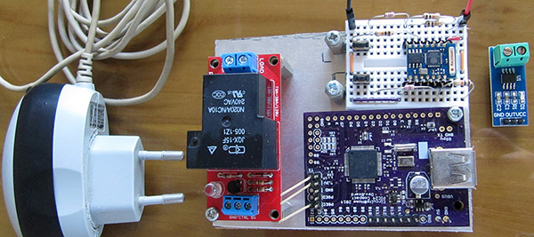
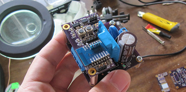
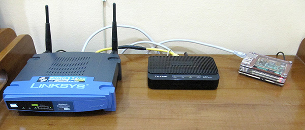
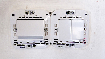
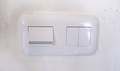
In the title picture you can see the result of my efforts. The physical switch consists of two wall wells – one containing the switch itself and the other containing its “brains” (seeing how it is a smart switch and all). The virtual interface is provided by OpenHab2 running on a RaspberryPi2.
Design/Features
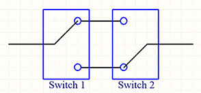
So where does one begin with the design of such a device? I wanted a something that would work in combination with the existing physical switch – not replace it, or be subject to an “override” where the physical switch has to be “on” in order for the virtual one to have any effect. There is a clever electrical construction to achieve this task, which is locally known as a “hotel switch”.
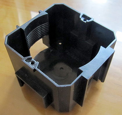
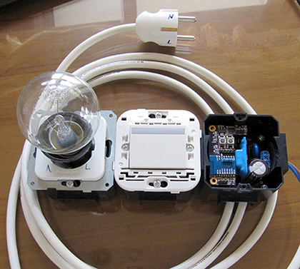
What about the physical form? I did not want anything that even remotely resembled a wall wart. I wanted my virtual switch to seamlessly blend with the physical switch so that nothing would give away its presence. This meant that the resultant PCB would have to fit into one of the common wall inserts that I found locally. The one in the picture is part of a line of Panasonic outlets/switches/etc so my switch would integrate into their lineup perfectly.
What about the “smart” functionality? I wanted a switch that would know whether it is on or not. Not just know the position of the relay, but actually know if there is current flowing through the system. Furthermore, I want this state to be remembered across, say, a power outage, so that lights don’t suddenly come on/off after power is restored.
Last, but certainly not least, I wanted a slick looking control panel to house the virtual switch interface. I needed a complete smarthome control solution into which I could integrate. I’ll be damned if I have to write another one-off app for the smartphone.
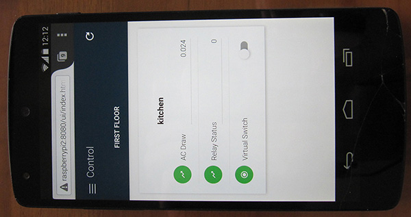
UI as seen on a Nexus 5
The First Prototype
So here I was, wanting to build a hardware gadget without knowing the first thing about doing so. I was familiar with programming microcontrollers, knew my way around a multimeter and I had previously soldered some fairly sophisticated boards of other people’s design, but design my own board? I’ve done nothing of the sort. To avoid making PCBs I decided to build the initial version of my switch from a set of loosely connected breakout modules. Here’s what I collected:
For 220 VAC to 5 VDC power transformation I would use a cellphone charger. Use a quality charger for this. Like one that originally came with some phone you bought. Don’t buy an after-market charger as they are usually of poor quality. I used an old Samsung charger.
For a relay, I ordered a “beefcake” relay kit from SparkFun. It was a giant 20A relay that made a loud clicking sound placed on a small PCB equipped with all the right periphery (transistor, reverse current protection diode, etc) to drive the relay from a microcontroller pin.
For current sensing I picked up one of Allegro’s ACS712 modules on a breakout board from ebay. It was conveniently laid out with all the necessary periphery, all I had to do was plug in +5VDC, GND and read the analog output.
The above made my power module. For the brains module I had this:
A PIC24F development board from Circuits@Home. It was built for making USB Host devices, but all I needed from it was the huge PIC it had on board. I purchased a Pickit3 programmer/debugger to use with it. Let me tell you, there is a special place in hell reserved for the person who first started calling that thing a debugger.
For the wifi module I had initially ordered a CC3000 breakout board from SparkFun. CC3000 was a wifi chip from TI Instruments that had all the potential to be wifi-enabled-washing-machine workhorse, until they jacked up the price for it from $10 to $30 and refused to give out any more samples. Luckily just before I sunk my teeth into it, another chip you may have heard about got released – the ESP8266. An ultra-affordable wifi chip, controlled by mysterious AT commands.
The AT-commands haunted me for some time. Why would someone implement such an arbitrary syntax? Then I finally realized that these AT commands were not proprietary to Espressif (the makers of ESP8266) who, in turn, used them because these same AT commands, in their exact eccentricity, have been used in similar products, such as GSM modems in the past (and before that in something else, and before that in something else still… all the way down to the original dial-up modem). The expectation was that people had already had libraries to parse these commands, which would make it easier to get started with the ESP8266. (Just not for me 😛 )
Controller Software
Now, programming was a different story. This I can do. Using this monteley crew of breakout boards I wrote the bulk of the microcontroller code. I had decided, somewhat arbitrarily, that my device would offer a JSON RPC interface over TCP. RPC (remote procedure call) seemed like the most logical way to organize the interaction with the smarthome control server. After initially connecting from the client (my device) to the server, the TCP socket would remain open and the server would call methods on the device such as ‘turn on’ or ‘turn off’ or ‘give status’ and receive back relevant data as a return value. Using JSON allowed me to use existing libraries for parsing of messages instead of having to implement my own syntax.
I found a small no-dependencies JSON library in C – JSMN. It was very straightforward to use, except offered no easy methods of the JSON tree traversal. No problem, it was quite easy to add. On top of this, I built my JSONRPC-server implementation: JSMN RPC. The module takes as an initialization argument an array of function pointers and name strings (kind of like registering JNI methods in Android) and then automatically executes these methods when it finds their names in the JSONRPC request. Automatic argument type checking is included, return type checking soon to be added. Take a look here if you’re interested.
Oh, one thing I should mention before getting too much further. Every microcontroller project should start with a good UART debug console. Sure, it’s easy to send some data over UART and then spin waiting for a reply, is that what you mean? No, that’s a bad UART console. A good UART console will be completely non-blocking, interrupt driven with ring-buffers and all. I could not find an open source version of such thing and was forced to port a vendor-locked version for my purposes. I keep telling myself that soon I will write my own version from scratch and release it, but so far, as you may have guessed, it hasn’t happened.
The last key piece of software that was necessary for bringing this all together was an interface to the ESP8266. I chose to implement this module as what I call an “at socket”. The user interface is socket-y: Open/Close/Send/Receive/JoinAP/QuitAP/etc, but behind the scenes these functions write appropriate AT commands to ESP’s UART, read responses and return binary-friendly status codes. This was actually quite a bit harder to write than it looks. Never having dealt with AT commands I didn’t know what, if any, conventions there were to begin with and which, if any, of those would be honored in this particular implementation. For example, there are no guidelines as to the synchronicity of the whole affair (can you inadvertently read an asynchronous command in the middle of a synchronous command/response sequence?). The control “phrases” vary across commands (eg. ERROR vs FAIL), and feature non EOL-terminated symbols (eg. ‘>’) so you can’t rely on just pulling lines from the UART buffer. And don’t forget that for receiving data one must parse out the message length as a string. Put together these make at-socketing a rather dreaded affair. In the end, through trial and error, I have arrived at something that works reliably, but you can probably imagine the internal structure of a module developed in this way. For that reason, don’t expect me to post that code here. Maybe in the future, once I get around to rewriting the whole thing with lessons-learned. I do have one question though – where are all those legacy AT parsing libraries that keep these AT commands alive?
Making PCBs
So far, I was able to compensate my lack of hardware design knowledge by using completed modules, but now it was staring me square in the face. The alpha version of the device code was ready and needed to be tried on real hardware. I knew it would take some time to make the PCBs, so I wanted to get the ball rolling right away and, in the meanwhile, work on the smarthome control server.
My queries about making this device towards an electronics guru friend were met with an absence of enthusiasm. I was on my own. I decided that I would at least draw the schematics. After all, I already had all the stand-alone modules, most of which came with schematics. All I needed to do was to unite everything into a single drawing. This would at least allow me to ask for help in a more serious manner.
With the help of youtube and web searching I was able to learn how to use CAD (I started with Eagle, and yes, it was awful). Initially, my goal was only to redraw the existing schematics into one big one, but inevitably, as I copied each piece I found myself wondering about how it does what it does. Usually I would get dizzy looking at a large schematic and my eyes would blur not even knowing where to begin. But here I had everything broken into small modules, small enough to be begin thinking about what each resistor/capacitor/etc does. I read and asked on stackoverflow and toster, and while I still had gaps in understanding, the many things started to make sense. Current limiting resistors, pull ups, pull downs, filtering caps, protection diodes, voltage dividers and so on. I also realized that for whatever chip, module and microcontroller that one wanted to use, the datasheet will usually contain an example schematic of how to wire it up. So even if you don’t fully understand how it works, you can start using it and asking questions. In this way I was even able to incorporate some elements into my schematic there were not present in the stand-alone modules. I was also finally able to narrow down the minimum circuit required to run a microcontroller about which I would like tell a side-story.
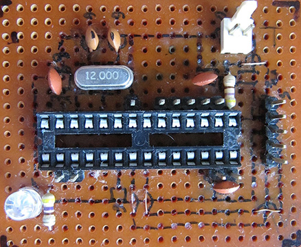
Right about the time I finished writing the first pass of the microcontroller code I had an unfortunate accident. While soaking my foot in a peroxide bath (jungle fungus, yuck, don’t ask) I failed to get up and pay attention while plugging in power to my test rig. As a result, I accidentally connected 12V as VCC. Magic smoke was released. As I pulled everything apart and checked each component individually, things looked bad. Everything burned out. The only thing that survived was the programmer, for which I was very grateful. Although, I was not certain of that at the time. This was a major bummer, but it only underscored the need to make my unified PCB. While I worked on finishing the schematic, I decided to try to make a new PIC24 devboard. I had a couple of chips and one of those prototyping “PCB”s and had already found the section in the datasheet that showed the minimal schematic. All I needed were the some ceramic capacitors, resistors, maybe a crystal and maybe a linear voltage regulator. I made a list and headed down to the local electronics store.
Let me tell you a little bit about Indonesian electronic stores. They usually consist of a dark, cramped room open to the street with minimal display space. Their best selling products are related to loudspeakers and audio amplification of various sorts for use in local mosques and some cheap Chinese LED contraptions that some like to attach to bumpers of their cars and motorcycles. All small electronic parts are stored in dusty stands behind the counter with faded drawer labels. Don’t even think about asking for a catalog – you say what you need and they’ll check if they have it or not. I logged on to Digikey, stared at the search box and cried that night. Once, I witnessed some school kids buying some LEDS, transistors and some other small stuff. I inquired as to what they were making, since this was the first time I had seen someone take an interest to raw electronics during my stay here. They told me that they were making a flip-flop. Suddenly I had hope! There is someone here who is interested in fundamental electronics! Maybe I could hire them when they graduate, or do a hackathon, or … well, let me tell you, the euphoria was short lived. It turned out that the only reason the students were making this flip-flop was for a school project and that their foray into the study of electronics would more or less begin and end there.
So, there I was, at one of these electronics stores with my list of parts. My request for ceramic capacitors was met with a blank stare. After 15 minutes of excruciating explanations I was able to walk out of the store with a 10K resistor, 12MHz crystal and 8nF ceramic caps for it. They had no other ceramics and had absolutely refused to accept my explanation of what a blank PCB looked like. It’s quite funny – you can describe something all day, but until you say the right keyword (‘PCB polos’) in the local jive all you get are blank stares.
My adventure would drag on for a few more weeks, until we visited the nearest “metropolis”. The shops there were a marginally better equipped, and having figured out the “keywords” I was able to quickly sample their selection. I was able to get some 0.1uF ceramics, but no larger. I was able to get a 10uF tantalum cap, but it would later turn out to be skunked and ruin my dev board. They also, gasp, had PCB polos! But only 1-sided. Sigh, you just can’t win, can you.
A few days later I soldered together my minimal dev board, using thin wire from a faulty transformer (which ironically came out of a soldering gun I bought locally) for tracks.
The moment of power-on was decidedly anti-climactic. The debugger would not connect to the chip. The cause was that faulty tantalum cap from above, but I would not figure that out until some time later. At this point I was still not sure if it was the debugger or I had put the dev board together wrong. To give you an end to this story – I later successfully recreated the minimal dev board on a breadboard with some gigantic thin film caps. This proved that the debugger was still alive.
Ok, where were we? I had finished drawing the schematics and was contemplating my next move. I did not want to do PCB layout myself. First of all, this would be my first board – that’s a guaranteed fuck up. Second of all, the power module involved 220V traces, for which, any fuck ups carried an additional risk of fire. So I did what any normal person would do – I placed a freelance order on freelansim.ru. I had three people reply, and that’s how I met Danil. He did an excellent job with both the power and logic modules. He even talked me into learning Altium, which is like Photoshop to Eagle’s MSPaint.
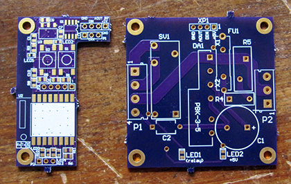
While Danil was working on the layout I helped by preparing some footprints and finalized the choice of main components. To satisfy my itch do some of the layout myself, I found a treasure trove of altium training videos (in addition to their awesome documentation). I recommend this guy (Fedevel Academy), his style resonated with me quite well. With my newfound knowledge I was able to examine the layouts Danil was producing and provide meaningful feedback. My point is – learn the CAD software, it’s easier than it seems. Running a little bit ahead, here’s a pic of the produced PCBs
Having the Gerber files in my grubby little hands, I had to find a place to produce the PCBs and source my components. I am aware of only two places that specialize on small PCB orders – oshpark and cheapdirtypcbs. I chose oshpark because I really like their automated Gerber submission software and I’ve seen their product and it is fantastic. The only problem is – they’re in the US and I am in Indonesia. Well, you know what’s an even bigger problem? Trying to freaking shop for components to be sent to Indonesia. There is no local presence of any of the big retailers like Digikey/Mouser/Element14/etc. I thought about ordering from one their other SEA outlets – Mouser has a Malaysian site, Element14 has a presence in Singapore. Good luck getting a shipping quote, though. I believe it was Mouser, who, on their Malaysian site proclaimed, in a 3-exlamantion-signs announcement, that now, they offer flat rate shipping to Indonesia!!! For the low, low price of $70. Ahem. Moving on. In the end, I found a re-shipper in the US who was able to receive my PCBs and components and send them to me. The international shipping was now $23. One month later, the package would arrive at my door. Anyone want to go in on starting an electronics components retailer with me in Indonesia? (Seriously).
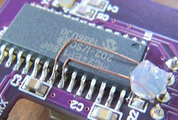
Having previously completed the “Indiana Jones and the Variable Temperature Soldering Gun” gauntlet (don’t even ask me about the chisel tips), I got to soldering. A few backwards diodes later, I had my power module going. The microcontroller module presented more challenges. It turned out that I had made the ESP8266 footprint as a mirror-image of how it should have been. 😳 I’m lucky it didn’t burn out being plugged in like that. Using a hot air gun I was able to de-solder the module, knocking off the antenna in the process. 😳 I then reattached it upside down, which worked pretty well.
The next adventure came from the linear power regulator. My 5V input from the power module was at the extreme low end of allowable input range, I don’t know how I missed that. So as soon as I would put a load on it (read – turn on ESP8266) the 3.3V line would sag to about 2.7V and trigger a brown out on the PIC. I immediately ordered a replacement regulator (MCP1825 – highly recommend) from AliExpress. AliExpress is actually very usable for individual components – similar price to what you’d pay in the US, free shipping, as long as you buy in some small quantity. Though I don’t really see myself shopping for a whole BOM, one transaction at a time.
The last bug in the logic board was my selection of pins for PIC-ESP8266 UART. I’ve been using Microchip’s remappable peripherals successfully, but failed to notice the fact that some of the remappable pins are only available for input. Of course, I had put both UART lines on such pins. Well, nothing an exacto knife and some thin wire can’t fix. I cut some traces and laid a “detour” over the top of the chip. Some hot glue to hold everything in place and we’re done.
It booted! I was able to run the full system through the paces, including reading some analog output from current sensor. I manually sent JSONRPC commands and got responses. Wifi and TCP connectivity were working. The assembled, second stage prototype now looks like this:
Smarthome control center
The smarthome control center is the most valuable piece of the whole smarthome universe. Control the server and you can: dictate which gadgets are and are not compatible (ultimate vendor lock in), funnel all metrics through your “cloud” server (and send baby food ads when you detect a single room being painted), integrate with some Corporation-Of-Evil (for an enhanced experience no doubt), or pull some other underhanded move in a captive market. So all you budding smart-homers, think long and hard about who you want handling the heart of your machine. Hopefully the answer you will come up with will be ‘yourself’, but these day I am not sure what to think anymore.
I quickly attempted to sample (install and launch) all the home automation solutions that I could find. This article has a decent list (at the very end), but honestly these days the control server solutions are growing like mushrooms after a fall rain so there are likely many more out there. But of those I examined I didn’t like *any*. The common themes were half dead development state, half-assed half-written documentation, sloppy security practices (web server based solution – all directories 777 owned by server process, exec()’s in page code), cloud tie-ins, and in all cases atrocious interfaces. I tried (within reason) to honestly launch each one and see how it looked in my environment. Some 50% did not even run. Of the remainder I settled on OpenHab because it had the most complete documentation, active development and a large-ish community. I also liked that it is written in Java. The drawbacks of OpenHab are: complexity of the code, fugly interface (much better now in OpenHab2), and lack of a good gathering place to ask questions. Currently, OpenHab2 is in alpha stages and offers a refactored class structure (much clearer than in OpenHab1) and an awesome new PaperUI which is served up as a web page and looks great on both phones and PCs. Furthermore, the hooks are all there for one to write their own UI, should one find self so adventurous.
OpenHab is organized into core, ui and bindings. A binding is like a driver for a particular device. OpenHab comes with a couple of generalized bindings like http or tcp, so I initially cosidered using them (as my device is fundamentally a TCP device) but quickly realized that their use is limited to only the simplest of cases, and if you want any degree of logic there is only one way to get that – write your own binding. I also have a few choice words about the “binding notation” ;).
Luckily for us, the binding code structure has been much improved between OpenHab1 and OpenHab2, and with a little bit of perseverance and some github searching I was quickly able to make sense of the “API” for a binding and wrote one for my device. My binding is capable of discovering new devices, keeping track of connects/disconnects and maintaining up-to-date device state information. I will write a more detailed post talking about the making of a binding, but for now let me just discuss the architecture in a more general sense.
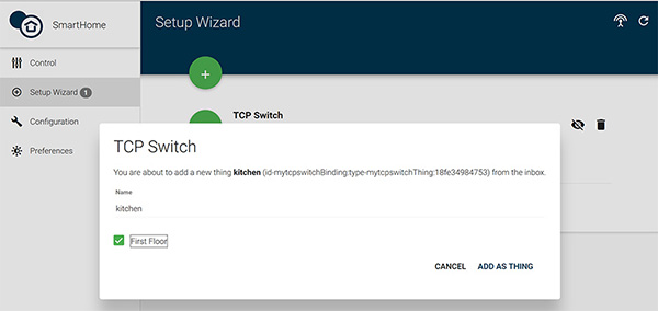
The OpenHab binary runs on any system with a Java VM and presents a web interface on the host. Our binding starts up listen a server over TCP and waits for any of the wifi switches to come online. The switch is initially programmed by the user with some basic parameters like wireless network name, password, and the hostname/ip where to look for the control server. Thus, as soon as it is able to join the wireless network, it will connect to the server ip and make contact with the binding. When this happens the user is notified via the UI that a new device was discovered and has a choice to add it to the control panel. That’s it – no config files or binding configuration strings. In the control panel it just looks like a switch, but wait, a it’s smart switch! Its state reflects the true state of the system. If you turn on the switch, but the bulb is burned out, it will quickly right itself back into the off position, since no current is flowing and whatever is behind the switch must be off.
Putting It All Together
After several iterations of “tweak binding-tweak microcontroller-tweak binding-tweak microcontroller” my system was ready to go live. Up to now I had been using this test rig, and running the OpenHab on the same machine where I was doing development.
The production environment is a Raspberry Pi2 running a compiled OpenHab2 distribution. The Pi is connected via a LAN cable to my general router (yup, still rocking a Wrt54G) and for extra security can put up its own access point so that the smarthome devices are isolated in their own network. Although, I have not done the latter yet. Here is what the control server looks like:
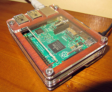
RaspberryPi2 in a stylish Zebra case
The “brain” of the smarthome.
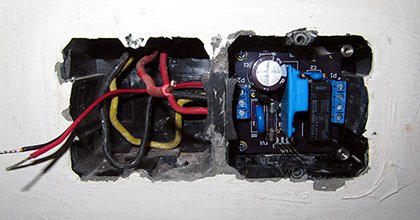
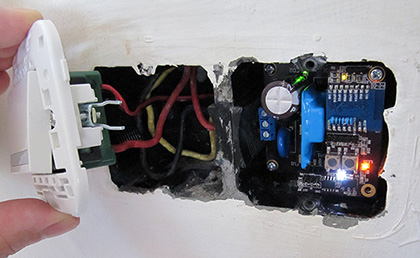
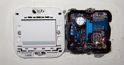
Now it was time to play electrician! Equipped with a tester screw driver (one with a light that goes one if you touch a live main) and a switched off breaker I tapped into the wiring. It is surprisingly hard to maneuver those thick solid copper wires around. Next, I present to you the assembly “time lapse”.
I’ve been running this setup for close to a week with good results, and am working on installing another wifi switch in a second location.
In conclusion
At this point my story comes to an end. I haven’t decided what to do next. My heart is nibbling at me to try applying to a hardware incubator with this as my project – after all, home automation is a trendy topic these days. My brain on the other hand, is telling that it’s just a hardware gadget and by itself is rather insignificant in the grand scheme of things. I would love to talk to anyone with relevant experience. Also, if I am to apply, I’d need to meet at least a hardware specialist and maybe a “peoples’ person”. Anyone want to join me?
Wow, I really mean WOW. This is a fantastic story. I am amazed by your ingenuity. I just wonder why you didn’t buy something off-the-shelf though. It would have been much cheaper and left you a lot of time to sit in the street and chat with the old men of the kampung. 🙂
Hi Rob, thank you for reading and for the comment!
To answer your question – I am not aware of a device with equivalent functionality, reasonable price and lack of a vendor lock-in. It seems like something completely mundane but there really are a lot of fine details that make or break such a device. My goal is two-fold: make something that I need myself, and try to market my switch to others – I like to think that I have a couple of good selling points 😉
What is relay use? sv1
hey, sorry for the late reply, I used an 8A Omron SPDT relay
I’m interesting to your smarthome, please contact my mail address. Terimakasih
Woww..it’s awesome dude..
Just curious to know..where do you live in somewhere as part of indonesia?wkwk..
Right now i also sticking on plan to automate my home. May i ask some if get problem? Thanks
Could I ask what IC are you using as AC/DC converter?
I mean DA1 on schematic diagram.
(from geektimes.ru)
Thank you in advance.
Hey, it’s a PBK-3-5 from CUI. May I ask what you’re building?
Hi.
Thank you. I found it.. it’s too expensive 🙁
I’m building project like yours.
But I’m using NRF24L01 + ATmega (or maybe change it to NRF69 or NRF905) instead of ESP8266.
And my “eternal problem” – small power supply 🙂
If you have some questions or something else – please email.
Thank you again.
Hey there, nice post ! I’m looking for ways to automate and integrate much of existing automation technology into one deplyobable solution
Like you, I reside in Indonesia and it’s ridiculously expensive to procure components from outside US. But hey if you are serious on doing this, drop me an email
Cheers,
Arief